
2023 BIO ASIA-Taiwan
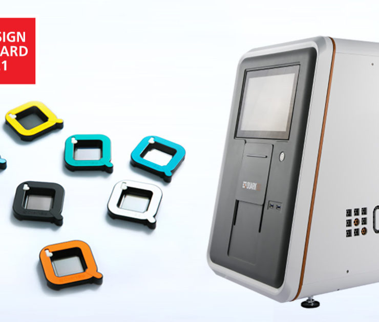
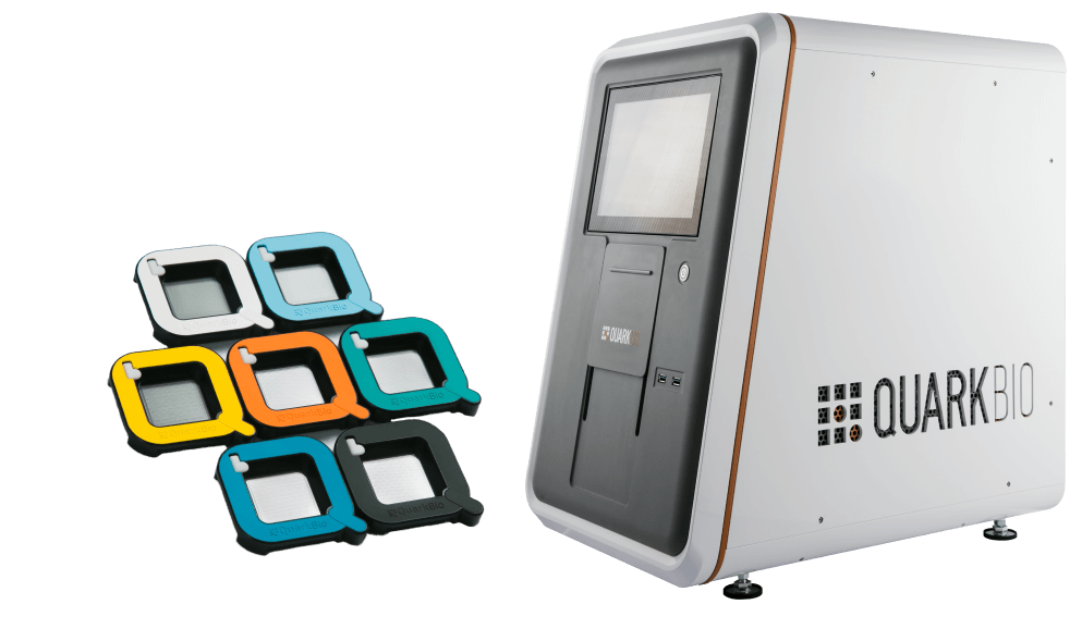
A Chip-based Clinically Oriented qPCR
NextAmp™ Analysis System
Virtual Exhibition
JUL 27 - JUL 30

Oncogenic Druggable Fusion
First line screening for possible fusion-targeted therapy
Indeterminate
Thyroid Nodule Cytology
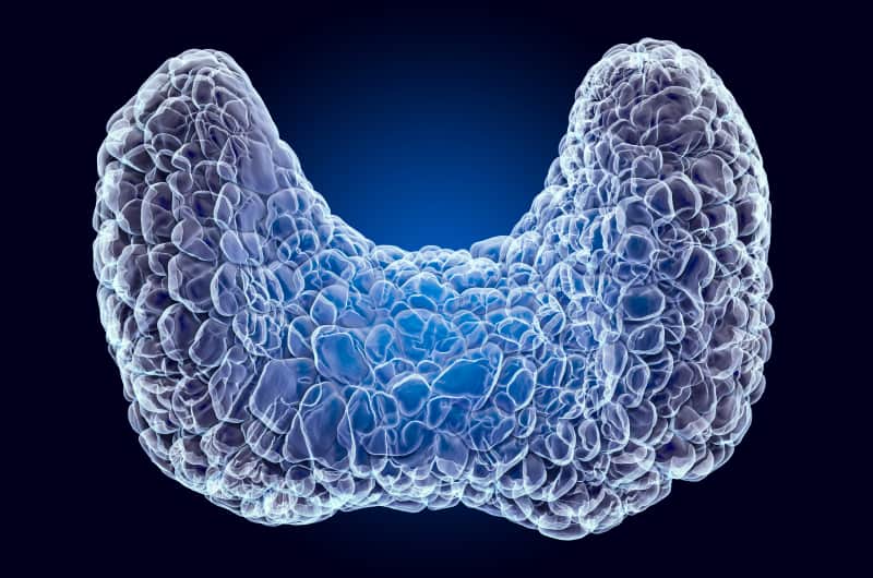
Solution: Risk stratification through fast, affordable molecular analysis
Insight to Action
Transform your research into clinical-actionable product

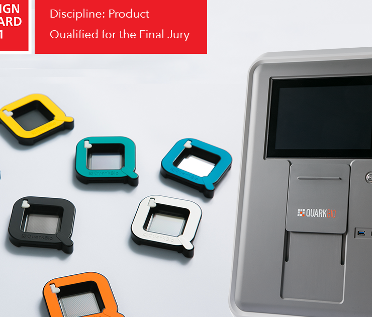
NextAmp™
Analysis System
A dual-functioning system capable of multi-biomarker analysis and digital detection of low quantity genes

Innovation through Collaborations
We collaborate for your success by customizing smarter and more suitable biomarker solution to meet your clinical needs

High Tolerance for Sample Quality
Our assays enable more patients to receive suitable drug treatments with the ability to analyze poor quality and low concentration samples

Pinpoint Eligible Patients
PanelChip® offers a cost-effective platform for large scale screening of patient with rare gene rearrangements

Proven Clinical Utility with Expression Biomarkers
Translating discoveries into products, we have helped multiple companies develop mRNA- and miRNA-based assay
What We Do
Simple to use cancer panels for actionable mutations and diagnosis

ThyroSCAN
Test for patient with suspicious thyroid nodules

FusionQuest
Test for cancer druggable fusions
Customized Services
Tailored-made Cancer Panels
Why QuarkBio?
Latest News
Events
BIO Asia-Taiwan 2023 Exhibition
BIO Asia-Taiwan 2023 Exhibition
CONFERENCE
Exhibition: Jul 27 – Jul 30,2023
Location: Taipei Nangang Exhibition Center,Hall 1,4F (M514)
Healthcare Expo | Taiwan
Healthcare Expo | Taiwan
CONFERENCE
Exhibition: Dec 01 – 04, 2022
Location: Taipei Nangang Exhibition Center, Hall 1, 1、4F (L003)
Publications
Learn more
